Thermal Desorption Spectroscopy (TDS) is mostly used to acquire information on the biding energies of molecules and atoms. The quantity and substance of a gas occurring in the vacuum process are analyzed by using the vacuum gage and the mass spectrometer. This technology enables the detection of the quantity change and the composition of a gas even in a minimal amount and the measurements of temporal change of the gas in each temperature in a vacuum device. Such features of the technology provide solutions for the quality improvement and the finding cause for an issue as well. The technology offers the best sensitivity for the analysis while allowing the analysis on any gas composition when using a mass spectrometer.
What is TDS?
TDS is a device that increases the temperature of a sample and measures and analyzes the gas separated from the sample. The device is used for the purpose to analyze and prevent the cause in advance by the qualitative and quantitative analyses of the gas released during a process.
Applications
– Material Analyses for Semiconductors and Displays
– Hydrogen Analyses on Automobile and Steel Materials
– Minimal Quantity Analyses of Ultra-Pure Materials
In general, the inspection for impurity (outgassing rate) due to the temperature increase is performed by using TDS. However, the local and direction oriented measurement and diagnose techniques on impurity mappings of wafers in real-time are not established until now while there is no system available for simultaneous qualitative and qualitative analyses. We supply the TDS, the product overcoming such disadvantages. Thermal desorption spectroscopy supplier Korea
Performance Comparisons
TDS by IVT possesses higher compatibilities on Calibration, Heating, Pumping Speed and others against that of other companies. Also, depending on the applied area, DAQ software convenient for users is provided.
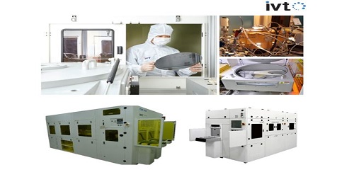
aTDS (Automated TDS for semiconductor Wafer)
aTDA includes EFEM and Wafer Transfer Robot for fully automated 300 mm wafer analysis and may be supplied in composition of various optional products for QMS on 100, 200, 300 ,500 amu and others. Wafer contamination scanner manufacturer
Specification
• •Sample Size: 300 mm WAFER
• •Halogen Lamp Heater
• •up to 950℃
• •High Vacuum with gold plated chamber
• •Fully Automatic (EFEM/Aligner/WTR)
TDS is a device that increases the temperature of a sample and measures and analyzes the gas TDS